Welcome to the official website of Hubei TrueLight 3D Sensing Technology Ltd.!


AMS Areal confocal 3D microscope
Technical Principle
Based on the principle of widefield microscopy, it utilizes structured light illumination to modulate the surface information of the object, removing out-of-focus signal interference. A 3D micro-surface topography is obtained through vertical axial scanning. It is suitable for both complex feature surfaces (such as scattering surfaces) and smooth surfaces. The Z-axis accuracy can be flexibly adjusted from 1nm to 1μm according to the application scenario.
World's first commercially available product with "array light + confocal imaging" technology | |
 | ● Unique areal light scanning confocal technology brings higher efficiency and stronger imaging capabilities ● Cross-scale, cross-material, cross-structure compatibility ● Integrating artificial intelligence to explore more application possibilities |
Schematic Diagram | |
Product Features
● New generation fully autonomous desktop confocal 3D microscope/profiler
● Surface scanning, cross-scale, true color, fast imaging
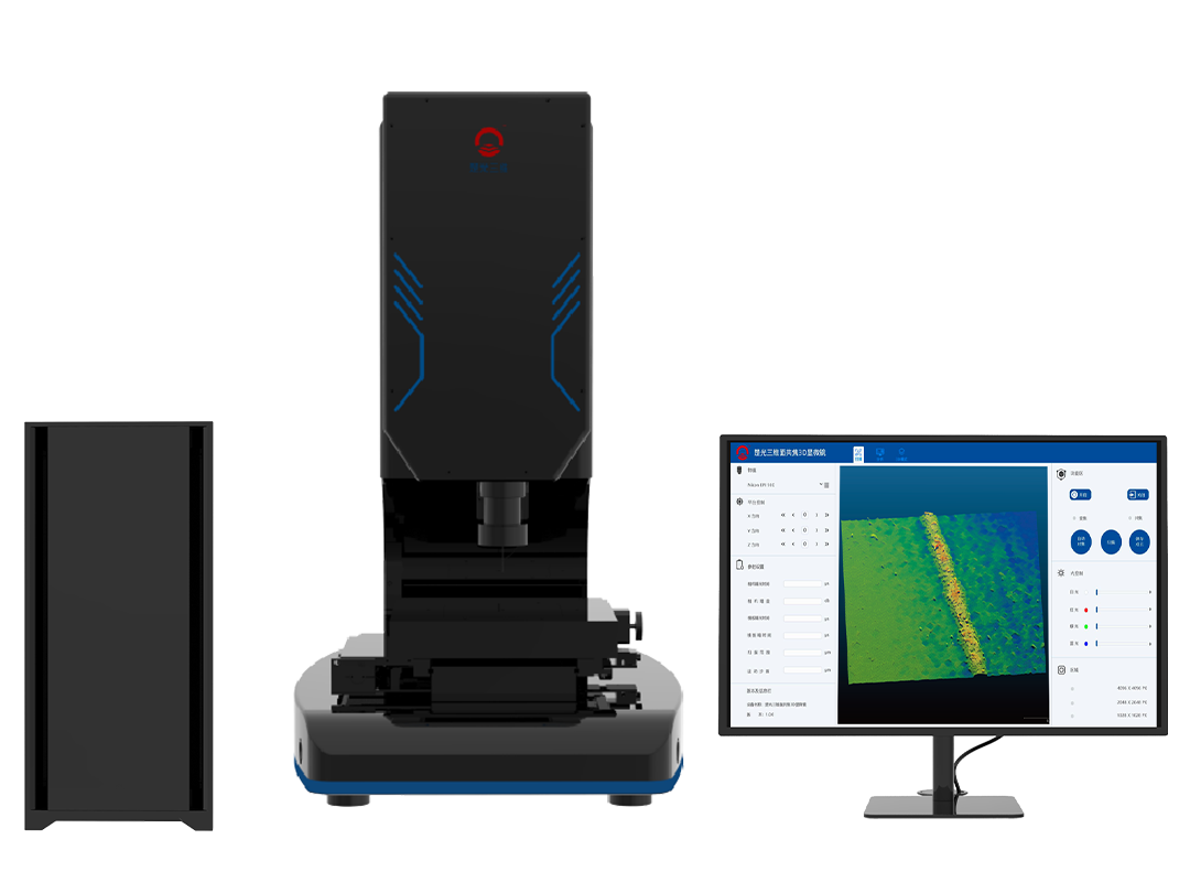 | Cross-scale compatibility:Compatible with high-precision mode (limit 1nm) and long-range (30mm), submicron precision mode High Adaptability:Adaptable to smooth surfaces, complex surfaces, highly reflective materials, and transparent materials Multifunctional:Measurement of roughness, warp/flatness, three-dimensional profile, size, XY large field of view stitching, surface image, etc. Low Maintenance Cost:LED light source, stable, reliable, and long lifespan Openness:Supports export of original true color images and 3D point clouds for convenient AI analysis |
| Confocal 3D Microscope Product Image |
Product Introduction
Cross-scale Application | ==> | 1 Confocal 3D Microscope = 1 Laser Confocal 3D Microscope + 1 Super-depth 3D Microscope | ||
Traditional Technology Products |
| Application Types | ||
①Super-depth Microscope Digital ②3D Microscope Laser Confocal ③3D Microscope White ④Light Interferometer | <==substitute | 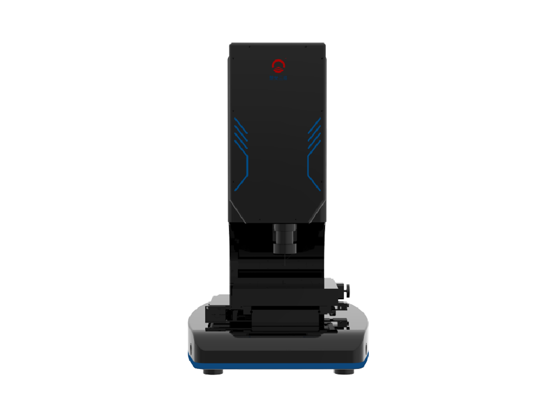 | applications==> | ①Defect observation and analysis ②Key dimension measurement ③Surface profile ④analysis Roughness detection ⑤Transparent film thickness detection... |
Model Name | AM 100 (Large Range) | AM 10 (High Precision) | AM 1 (Ultra-high Precision) | |||||||||||||||||||||||||||||||||||
Principle | White light confocal | White light confocal | White light confocal | |||||||||||||||||||||||||||||||||||
Axial Scanning Device | Motor | PZT+motor | PZT+motor | |||||||||||||||||||||||||||||||||||
Axial accuracy(μm) | 0.1 | 0.01 (PZT), 0.1 (Motor) | 0.001 (PZT), 0.1 (Motor) | |||||||||||||||||||||||||||||||||||
Range μm① | 30000 | 500 (PZT), 30000 (Motor) | 400 (PZT), 30000 (Motor) | |||||||||||||||||||||||||||||||||||
XY Stage mm② | 100 x 100 | 100 x 100 | 100 x 100 | |||||||||||||||||||||||||||||||||||
Size (HxWxD) mm | 780 x 475 x 595 | 780 x 475 x 595 | 780 x 475 x 595 | |||||||||||||||||||||||||||||||||||
Weight (kg) | 55 | 55 | 55 | |||||||||||||||||||||||||||||||||||
Optional Objective③ |
| |||||||||||||||||||||||||||||||||||||
Note | ①Limited by the objective lens working distance, the maximum range is 30mm; motor stroke 100mm; ②Can be customized according to requirements, supporting size matching, such as 12-inch wafers; ③Objective lens is not standard; select objective lens according to usage needs; ④A complete microscope includes a measuring head, objective lens, base, controller and display, measurement software, gauge blocks, among which the objective lens and gauge blocks are optional. | |||||||||||||||||||||||||||||||||||||
Key words:
Solar cell silicon suede pyramid, grid line measurement
PV application: Solar cell silicon suede pyramid, grid line measurement

High-end IC carrier bore hole depth measurement
High-end PCB manufacturing:Laser drilling of IC substrate application: High-end IC carrier bore hole depth measurement

Back bore hole depth measurement, up to 8mm deep hole
High-end PCB manufacturing:back drilling Application: Back bore hole depth measurement, up to 8mm deep hole

Measurement of the depth and width of the cutting groove after the wafer laser cutting
OSAT (Front-End) application: Measurement of the depth and width of the cutting groove after the wafer laser cutting

AMS Areal confocal 3D microscope
New generation fully autonomous desktop confocal 3D microscope/profiler
AM Areal confocal 3D microsensor
New generation fully autonomous confocal 3D microscopic sensor/probe

